Product Service

Compound Semiconductor Materials

Compound semiconductor is a type of semiconductor material composed of compounds. Compared with the widely used semiconductor material Si, wide band gap (WBG) compound semiconductors have superior material characteristics such as high voltage resistance, high current resistance, high heat dissipation efficiency, and high operating frequency, which have gradually attracted attention. Representative WBG materials are silicon carbide (SiC) and gallium nitride (GaN), which have the advantages of improving energy efficiency and reducing conversion loss in power electronics and 5G high-frequency applications.

We provide the following products:

SiC Crystal Grower (HTCVD/PVT)

SiC Crystal Grower (HTCVD/PVT)

Due to the specification of high temperature and stable, Single Silicon Carbide are usually used for semiconductor field. Nowadays, High-Temperature Chemical Vapor Deposition(HTCVD) and Physical Vapor Transport(PVT) are common in the SiC crystal growing method. These two method are available for mass production.

SiCube is used with HTCVD and PVT method for mass production.

 
Technical Data
  1. Diameter:4 inch
  2. Pressure : 5 – 900 mbar
  3. Temperature : 2600 °C
  4. Electric Power : 80kw
  5. Electric Frequency : 6~8 kHz
  6. Size : 2000 x 2500 x 3725 mm
  7. Weight(total) : 3800kg


baSiC-T is used to mass production for 4-6 inch diameter crystal with HTCVD method.


Technical Data 
 
  1. Diameter:4 ~6 inch
  2. Pressure : 1 – 900 mbar
  3. Temperature : 2600 °C
  4. Electric Power : 60 kw
  5. Electric Frequency : 6~12 kHz
  6. Size : 2000 x1200 x 2800 mm
  7. Weight(total) : Approx. 2000kg

Video Reference: 

* Please contact us for more product details.

Substrate

SiC wafer (substrate)

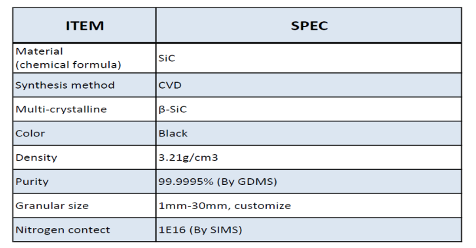
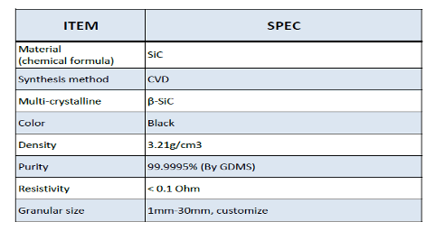
Silicon carbide (SiC), also known as carborundum, is a compound of silicon and carbon with chemical formula SiC.SiC is a Ⅳ-Ⅳ compound semiconductor material, with a variety Allotropic. The typical structure of which is divided into two types, first type is sphalerite crystal structure as 3C-SiC (β-SiC),second type is wurtzite hexagonal crystal structure; typically a 6H-SiC, 4H-SiC and 15R-SiC known as α-SiC. The most commonly used in the semiconductor industry are 4H-SiC and 6H-SiC structures.

There are some advantages for SiC:
–Current density can easily reach 5 or even 10 A/mm² (less than 1 A/mm² for silicon)
–Breakdown voltage (Volt/μm of epilayer) is typically in the 100 V/μm range for SiC, compared to 10 V/μm for silicon
–A single SiC device will drive higher current and voltage in a reduced foot-print.
–SiC is intrinsically very thermally conductive. Where a Silicon device will have to be cooled down to not exceed 85 °C, a similar SiC device will operate at 250°C with no degradation. This robustness to higher operation temperature will allow cost savings at system or module level where the cooling features (air, water, fans, heat sinks…) will be considerably reduced and shrunk.

•Higher electron mobility of SiC also permits higher frequency operation in switching mode.

Latentek can provide high quality single crystalline Silicon carbide wafer; furthermore, we provide two forms of wafer: semi-insulating and conductive as to meet the customer needs of high-frequency components and high power components. Current technical ability is able to provide MPD< 1 specifications of the wafer.

 
SiC Wafer Specification


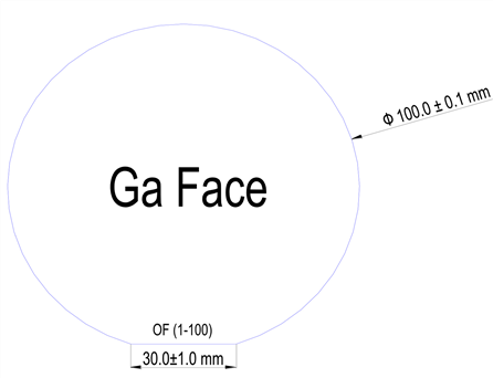
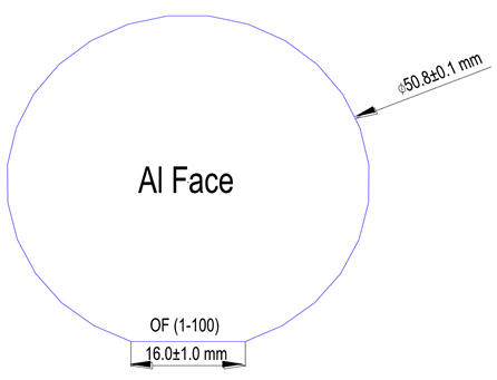
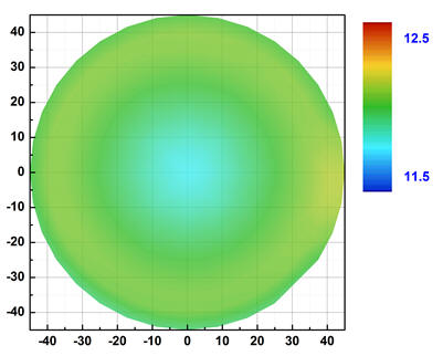
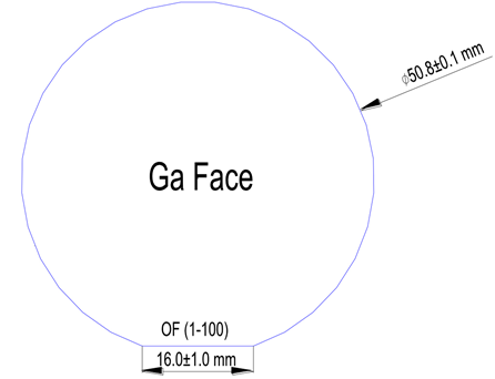
4-inch Specifications of 4H-SiC  High-Purity Semi-Insulating Substrate
PropertyProduction gradeResearch gradeDummy grade
Diameter100.0mm+0.0/-0.5mm
Surface Orientation{0001}±0.2°
Primary Flat Orientation<11-20>±5.0°
Secondary Flat Orientation90.0° CW from Primary Flat ±5.0°, Si Face up
Primary Flat Length32.5mm±2.0mm
Secondary Flat Length18.0mm±2.0mm
Wafer EdgeChamfer
Micro Pipe Density≦5micropipes/cm 2≦10micropipes/cm 2≦50micropipes/cm 2
Polytype Area by High-intensity LightNone≦10% of Whole Area
Resistivity≧ 1E7Ω‧cm(Area75%) ≧ 1E7Ω‧cm
Thickness500.μm±25.μm or 350.0μm±25.μm
TTV≦10μm≦15μm
Bow (Absolute Value)≦25μm≦30μm
Warp≦45μm
Surface RoughnessSi-Face CMP Ra ≦0.5nmN/A
Cracks by High-intensity LightNone
Edge Chips/Indents by Diffuse LightingnoneQty. ≦2, the length and width of each<1.0mm
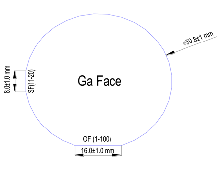
4-inch Specifications of 4H-SiC N-type Substrate
Product performanceU levelP gradeR gradeClass D
diameter100.0mm+0.0/-0.5mm
Surface orientationCrystal orientation: 4°, <11-20>±0.5°
Primary reference plane orientation<11-20>±5.0°
Secondary reference plane orientationClockwise 90°±5.0° with the main reference surface, Si face up
Length of main reference surface32.5mm±2.0mm
Length of secondary reference surface18.0mm±2.0mm
Chip edgeChamfer
Microtubule density≦1pcs/cm 2≦5pcs/cm 2≦10pcs/cm 2≦50pcs/cm 2
PolytypeNot allowedCumulative area≦10%
Resistivity0.015Ω ‧ cm~0.028Ω ‧ cm(75% area) 0.015Ω‧cm
~0.028Ω ‧ cm
thickness350.0μm±25.0μm or 500.0μm±25.0μm
Total thickness change≦10μm≦15μm
Deflection value (absolute value)≦25μm≦30μm
Warpage≦45μm
Surface treatmentC-side: optical polishing; Si-side: chemical mechanical polishing (CMP)
Surface roughnessSi-surface CMP Ra≦0.5nmN/A
Crack (observed by strong light)Not allowed
Edge collapse/notch
(observation of diffuse reflection light)
Not allowed≦2, and each length and width are <1.0mm
6-inch Specifications of 4H-SiC N-type Substrate
Product performancestandard
diameter150.0mm±0.25mm
Surface orientationCrystal orientation: 4°, <11-20>±0.5°
Primary reference plane orientation<11-20>±5.0°
Secondary reference plane orientationN/A
Length of main reference surface47.5mm±2.0mm
Length of secondary reference surfaceN/A
Chip edgeChamfer
Microtubule density≦5pcs/cm 2
PolytypeNot allowed
Resistivity0.015Ω ‧ cm~0.028Ω ‧ cm
thickness350.0μm±25.0μm
Total thickness change≦10μm
Deflection value (absolute value)≦40μm
Warpage≦60μm
Surface treatmentDouble-sided polishing; Si surface CMP
Crack (observed by strong light)Not allowed
Edge collapse/notch
(observation of diffuse reflection light)
Not allowed

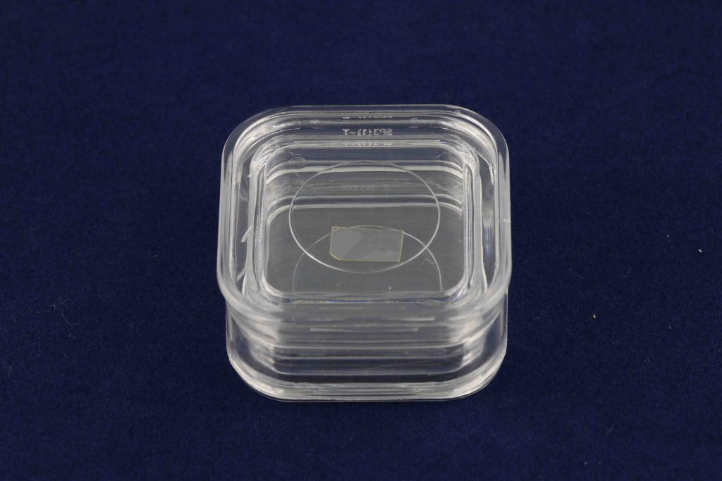
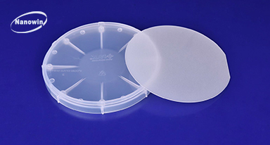
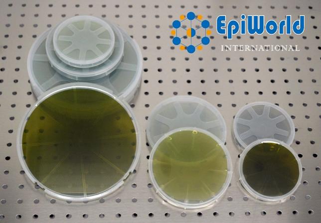
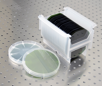
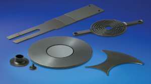
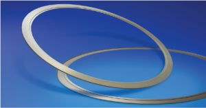
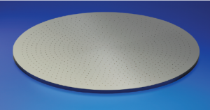
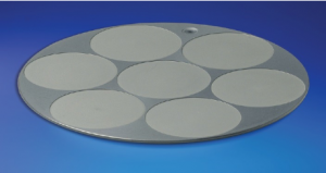
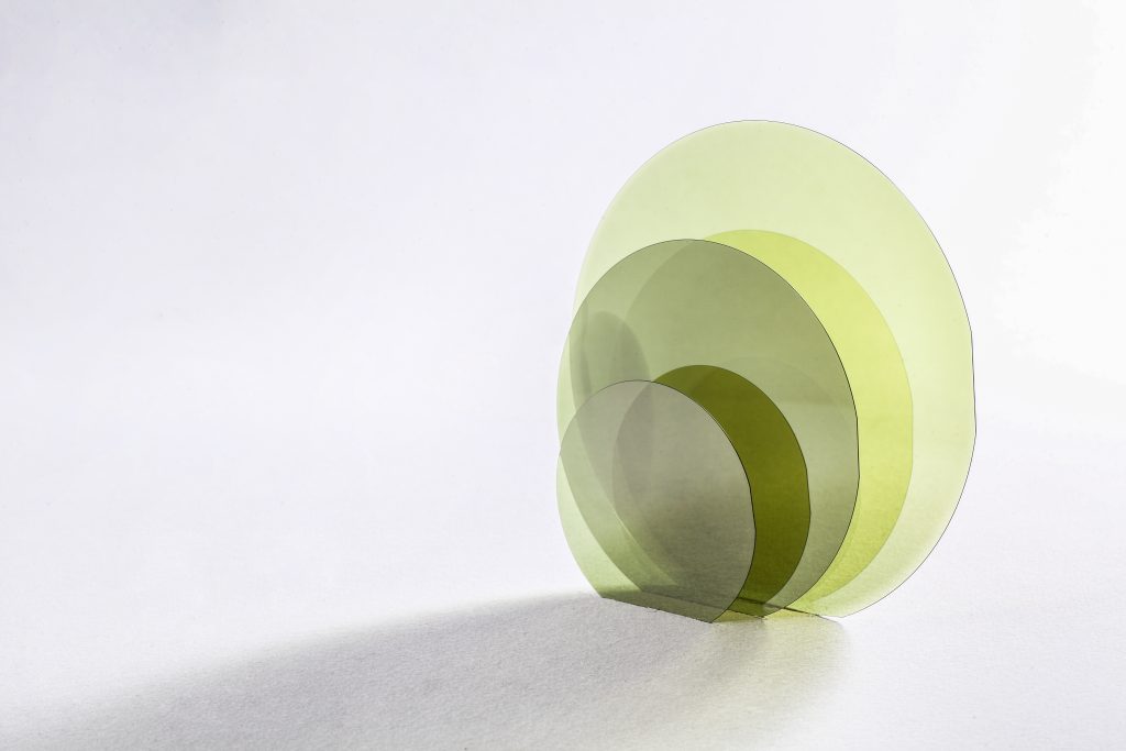
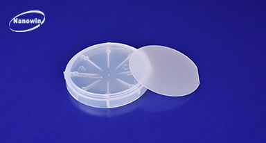
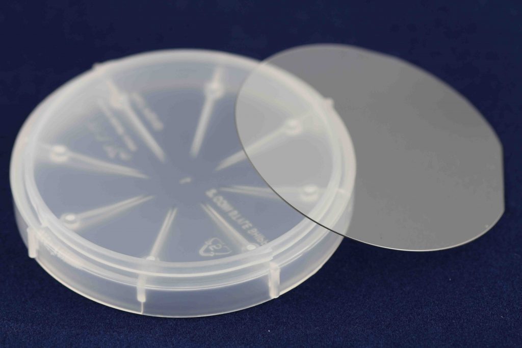
(2) Physical display of silicon carbide wafers

* If there are other specifications needs, please contact us to discuss.

GaN


GaN Substrates

 
2 inch GaN Template


Product numberGaN-TCU-C50GaN-TCN-C50GaN-TCP-C50
sizeФ50.8 ± 0.1 mmФ50.8 ± 0.1 mmФ50.8 ± 0.1 mm
thickness4.5±0.5 µm, 20±2 µm4.5±0.5 µm, 20±2 µm4.5±0.5 µm
Crystal orientationC-plane(0001) ± 0.5°C-plane(0001) ± 0.5°C-plane(0001) ± 0.5°
Conductivity typeN-type(Undoped)N-type(Si-doped)P-type(Mg-doped)
Resistivity (300 K)<0.5Ω·cm<0.05Ω·cm~10Ω·cm
Carrier concentration<5×10 17 cm -3> 1×10 18 cm -3> 6×10 16 cm -3
Mobility~ 300cm 2 /V•s~ 200cm 2 /V•s~ 10cm 2 /V•s
Dislocation densityLess than 5×10 8  cm -2 (estimated by FWHMs of XRD)Less than 5×10 8  cm -2 (estimated by FWHMs of XRD)Less than 5×10 8 cm -2 (estimated by FWHMs of XRD)
Substrate structureGaN on sapphire (standard :SSP option:DSP)GaN on sapphire (standard :SSP option:DSP)GaN on sapphire (standard :SSP option:DSP)
Effective area>90%>90%>90%
packagePackaged in a class 100 clean room environment, in cassette of 25pcsPackaged in a class 100 clean room environment, in cassette of 25pcsPackaged in a class 100 clean room environment, in cassette of 25pcs
or single container, under a nitrogen atmosphere.or single container, under a nitrogen atmosphere.or single container, under a nitrogen atmosphere.


2 inch Free-Standing GaN Substrate

Product numberGaN-FS-CU-C50GaN-FS-CN-C50GaN-FS-C-SI-C50
sizeФ 50.8 ± 1 mmФ 50.8 ± 1 mmФ 50.8 ± 1 mm
thickness350 ± 30 µm400 ± 30 µm350 ± 30 µm
Effective area>90%>90%>90%
Crystal orientationC-plane (0001) off angle toward M-Axis 0.35°± 0.15°C-plane (0001) off angle toward M-Axis 0.35°± 0.15°C-plane (0001) off angle toward M-Axis 0.35°± 0.15°
Main positioning edge(1-100)±0.5°, 16.0±1.0mm(1-100)±0.5°, 16.0±1.0mm(1-100)±0.5°, 16.0±1.0mm
Secondary positioning edge(11-20)±3°,8.0±1.0mm(11-20)±3°,8.0±1.0mm(11-20)±3°,8.0±1.0mm
TTV15µm15µm15µm
Curvature20µm20µm20µm
Conductivity typeN-typeN-typeSemi-Insulating
Resistivity
(300 K)
<0.5Ω·cm<0.05Ω·cm> 10 6  Ω·cm
Dislocation densityFrom 1×10 5  to 3×10 6  cm -2From1x105 to3x106 cm-2From1x105 to 3×106 cm-2
PolishingFront surface:Ra<0.2 nm(polished);Front surface:Ra<0.2 nm(polished);Front surface:Ra<0.2 nm(polished);
or<0.3nm (polished and surface treatment for epitaxy)or<0.3nm (polished and surface treatment for epitaxy)or<0.3nm (polished and surface treatment for epitaxy)
Back Surface:0.5~1.5μm;Back Surface:0.5~1.5μm;Back Surface:0.5~1.5μm;
option:1-3nm (Fine ground); < 0.2nm(polished)option:1-3nm (Fine ground); < 0.2nm(polished)option:1-3nm (Fine ground); < 0.2nm(polished)
packagePackaged in a class 100 clean room environment,Packaged in a class 100 clean room environment,Packaged in a class 100 clean room environment,
 in single container,under a nitrogen atmosphere. in single container,under a nitrogen atmosphere. in single container,under a nitrogen atmosphere.


10×10.5mm2 Free-Standing GaN Substrate


Product numberGaN-FS-C-U-S10GaN-FS-C-N-S10GaN-FS-C-SI-S10
Dimensions10×10.5mm210×10.5mm210×10.5mm2
Thickness350±30μm400±30μm350±30μm
OrientationC-plane(0001)off angle toward M-Axis 0.35°±0.15°C-plane(0001)off angle toward M-Axis 0.35°±0.15°C-plane(0001)off angle toward M-Axis 0.35°±0.15°
TTV10µm10µm10µm
BOW10µm10µm10µm
Conduction TypeN-typeN-typeSemi-Insulating
Resistivity(300 K)< 0.5Ω·cm< 0.05Ω·cm> 106Ω·cm
Dislocation DensityFrom 1×10⁵ to 3×106cm-2From 1×10⁵ to 3×106cm-2From 1×10⁵to 3×106cm-2
Useable Surface Area>90%>90%>90%
PolishingFront Surface:Ra<0.2 nm(polished);Front Surface:Ra<0.2 nm(polished);Front Surface:Ra<0.2 nm(polished);
or <0.3nm(polished and surface treatment for epitaxy)or <0.3nm(polished and surface treatment for epitaxy)or <0.3nm(polished and surface treatment for epitaxy)
Back Surface:0.5~1.5μm;Back Surface:0.5~1.5μm;Back Surface:0.5~1.5μm;
option:1-3nm(Fine ground);<0.2nm(polished)option:1-3nm(Fine ground);<0.2nm(polished)option:1-3nm(Fine ground);<0.2nm(polished)
PackagePackaged in a class 100 clean room environment,Packaged in a class 100 clean room environment,Packaged in a class 100 clean room environment,
 in single container,under a nitrogen atmosphere. in single container,under a nitrogen atmosphere.iin single container,under a nitrogen atmosphere.


Non-Polar and Semi-Polar Free-Standing GaN Substrate


Product numberGaN-FS-A-U/N/SI-SGaN-FS-M-U/N/SI-SGaN-FS-SP-U/N/SI-S
Dimensions(5.0~10.0)× 10.0 mm2(5.0~10.0)× 10.0 mm2(5.0~10.0)× 10.0 mm2
(5.0~10.0)× 20.0mm2(5.0~10.0)× 20.0mm2(5.0~10.0)× 20.0mm2
Thickness350±25μm350±25μm350±25μm
Plane(11-20)(1-100)(20-21)
(20-2-1)
(11-22)
(10-11)
Miscut Angle-1°±0.2°-1°±0.2°-1°±0.2°
TTV10µm10µm10µm
BOW10µm10µm10µm
Conduction TypeN-type  < 0.1Ω·cmN-type  < 0.1Ω·cmN-type  < 0.1Ω·cm
Resistivity(300 K)N-type < 0.05Ω·cmN-type < 0.05Ω·cmN-type < 0.05Ω·cm
 Semi-Insulating > 106Ω·cmSemi-Insulating > 106Ω·cmSemi-Insulating > 106Ω·cm
Dislocation DensityFrom 1×10⁵ to 3×106cm-2From 1×10⁵ to 3×106 cm-2From 1×10⁵ to 3×106 cm-2
Useable Surface Area>90%>90%>90%
PolishingFront Surface:Ra<0.2 nm(polished);Front Surface:Ra<0.2 nm(polished)Front Surface:Ra<0.2 nm(polished)
Back Surface:1-3nm(fine ground);Back Surface:1-3nm(fine ground);Back Surface:1-3nm(fine ground);
option:<0.2nm(polished)option:<0.2nm(polished).option:<0.2nm(polished).
PackagePackaged in a class 100 clean room environment,Packaged in a class 100 clean room environment,Packaged in a class 100 clean room environment,
 in single container,under a nitrogen atmosphere.in single container,under a nitrogen atmosphere.in single container,under a nitrogen atmosphere.
 
 
4 inch GaN Template

 
Product numberGaN-T-C-U-C100GaN-T-C-N-C100
DimensionsФ 100 ± 0.1 mmФ 100 ± 0.1 mm
Thickness4.5±0.5 µm, 20±2 µm4.5±0.5 µm, 20±2 µm
OrientationC-plane(0001) ± 0.5°C-plane(0001) ± 0.5°
Conductivity typeN-type(Undoped)N-type(Si-doped)
Resistivity (300 K)<0.5Ω·cm<0.05Ω·cm
Carrier concentration<5×10 17 cm -3> 1×10 18 cm -3
Mobility~ 300cm 2 /V•s~ 200cm 2 /V•s
Dislocation densityLess than 5×10 8  cm -2 (estimated by FWHMs of XRD)Less than 5×10 8  cm -2 (estimated by FWHMs of XRD)
Substrate structureGaN on sapphire (standard :SSP option:DSP)GaN on sapphire (standard :SSP option:DSP)
Effective area>90%>90%
PackagePackaged in a class 100 clean room environment, in cassette of 25pcsPackaged in a class 100 clean room environment, in cassette of 25pcs
or single container, under a nitrogen atmosphere.or single container, under a nitrogen atmosphere.


AIN

2 inch AlN Template

Product number AlN-TC-C50
size Ф 50.8 ± 0.1 mm
thickness 4±1.5µm
Crystal orientation C-plane (0001)
Conductivity type Semi-Insulating
Crystal quality XRD FWHM of (0002) <350 arcsec
XRD FWHM of (1012) <450 arcsec
Surface roughness Ra <5 nm (10 x 10 µm 2 )
Substrate structure AlN on sapphire (SSP)
Effective area Exclusion zone< 2 mm
package Packaged in a class 100 clean room environment, in cassette of 25pcs
or single container, under a nitrogen atmosphere.

SiC epi-wafer

SiC on SiC

SiC Epitaxial Wafer


SiC epitaxial wafer are used in a variety of electronic components such as: Shockley Diodes, MOSFET, JFET, BJT, Thyristor, GTO and IGBT. Please refer to our 4″~6″ SiC specifications or contact us directly.


4H-SiC Epi-Wafer Standard Specification (150mm & 100mm & 76.2mm)

Substrate orientation : Epitaxy is only available for off-axis substrates
Doping
 n-typep-type
DopantNitrogenAluminum
Net Doping DensityND-NANA-ND
Silicon Face9E14~1E19cm-39E14~1E19cm-3
Tolerance± 15%± 50%
Uniformity≦ 10%≦ 20%
Thickness: 0.2~100µm
Tolerance± 10%
Uniformity≦ 5%

CharacteristicsAcceptable LimitsDefinitionsTest Methods
Epi Defects2mm*2mm
die yield  95%
Defects only include triangular defects, downfalls, carrots and comets.candela CS920
Edge Chips≦ 2 with radius 1.5mmAreas where material has been unintentionally peeled off from the waferHigh Intensity illumination
Scratches≦ 10 lines total and the total length of these lines should be less than wafer diameterGrooves or cuts below the surface plane of the wafer having a length-to-width ratio of greater than 5 to 1
Surface Roughness<0.5mm20µm*20µm scanned by AFM
Backside Cleanliness100% cleanNone contamination
Thicknesssee specification tableThickness is determined as an average value across the wafer by FTIRFTIR
Net dopingsee specification tableNet doping  is determined as an average value across the wafer by MCV.MCV


SiC Epi-Wafer thickness Uniformity Distribution Chart

mean value(µm):12.04
sigma/mean:1.28%
(max-min)/(max+min):3.04%


SiC Epi-Wafer Doping Unformity Distribution Chart

mean value(cm-3):7.9515
sigma/mean:3.48%
(max-min)/(max+min):9.97%

GaN on SiC

If you have any related requirements, please feel free to contact us, and we will ask someone to evaluate and quote for you.

CVD SiC

CVD SiC

CVD SiC Bulk Synthesis

Feature:

Ultra-pure 99.999% (by GDMS)

• Outstanding corrosion resistance in plasma applications

• Proven durability in high temperature ammonia environments

• Excellent thermal shock resistant

• High thermal conductivity

• Excellent stiffness to weight ratio

• Fine grained microstructure

Non-porous

SiC bulk material for semi-tool(high-temp., high-erosion environment)

Raw material for SiC crystalline growth

High purity CVD SiC Parts for Semiconductor

High temp., high erosion

Rapid thermal process, etching rings

Plasma etching

MOCVD

High purity CVD SiC Granular for Crystal Growth | Customize Size

Silicon Carbide (Low Nitrogen)

Silicon Carbide (Standard)

Copyright © 2020  Latent Technologies Inc. | 磊拓科技股份有限公司

Address: 10th Floor, No. 86-3, Yiwen 1st Street, Taoyuan District, Taoyuan City, TAIWAN

TEL:  + 886 3-3589738

Scroll to Top